(Hong Kong)

Product Summary
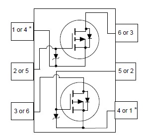
The FDG6304P is a P-Channel logic level enhancement mode field effect transistor. It is produced using the high cell density, DMOS technology. This very high density process is especially tailored to minimize on-state resistance. The FDG6304P has been designed especially for low voltage applications as a replacement for bipolar digital transistors and small signal MOSFETs.
Parametrics
FDG6304P absolute maximum ratings: (1)VDSS Drain-Source Voltage: -25 V; (2)VGSS Gate-Source Voltage: -8 V; (3)ID Drain/Output Current - Continuous: -0.41 A; - Pulsed: -1.5A; (4)PD Maximum Power Dissipation: 0.3 W; (5)TJ,TSTG Operating and Storage Temperature Range: -55 to 150 ℃; (6)ESD Electrostatic Discharge Rating MIL-STD-883DHuman Body Model (100 pF / 1500 Ω): 6.0 kV.
Features
FDG6304P features: (1)-25 V, -0.41 A continuous, -1.5 A peak. RDS(ON) = 1.1 Ω @ VGS= -4.5 V, RDS(ON) = 1.5 Ω @ VGS= -2.7 V; (2)Very low level gate drive requirements allowing direct operation in 3 V circuits (VGS(th) < 1.5 V); (3)Gate-Source Zener for ESD ruggedness(>6kV Human Body Model); (4)Compact industry standard SC70-6 surface mount package.
Diagrams
| Image | Part No | Mfg | Description |  |
Pricing (USD) |
Quantity | ||||||||||||
|---|---|---|---|---|---|---|---|---|---|---|---|---|---|---|---|---|---|---|
 |
 FDG6304P |
Fairchild Semiconductor |
MOSFET SC70-6 P-CH -25V |
Data Sheet |
|
|
||||||||||||
|
FDG6304P_D87Z |
Fairchild Semiconductor |
MOSFET SC70-6 P-CH -25V |
Data Sheet |
Negotiable |
|
||||||||||||
 |
FDG6304P_Q |
Fairchild Semiconductor |
MOSFET SC70-6 P-CH -25V |
Data Sheet |
Negotiable |
|
||||||||||||